XTB-IIR Assembly Notes
09/20/16
Please check for the latest version before beginning assembly.
Note: These assembly notes are for PCB version 1.31 or 1.32. Please contact me if you need assembly notes for the prior PCB version.
PCB versions 1.31 and 1.32 are almost identical and function the same as prior versions. There have been several minor changes:
1) Higher voltage components have been used in the powerline interface since version 1.30 to prevent damage if the neutral connection is not connected properly.
2) A logic level power FET has been used since version 1.30 to simplify the driver stage. It requires a slightly different version of the firmware that freed up a pin for a mode select jumper. That is only used for testing, and the jumper should normally be installed.
3) Version 1.31 added a second jumper to allow it to share firmware with earlier units. Since that jumper routes the drive signal to the power stage, it MUST be placed in the position that matches the firmware version to prevent damage.
4) The unused diode footprints on the 1.3 PCB were eliminated, allowing several components to be moved further apart for easier assembly.
5) Version 1.32 added C4A so 0.47uF 250V and 0.1uF 250V capacitors can be substituted for the 0.56uF 200V capacitor that doubled in cost to $9. Additional pads were added at the large inductor L3 to also accommodate alternate components.
The XTB-IIR has a densely populated circuit board. Some locations are left unpopulated in the single-output 240V 50Hz version. Assembly requires experience working with small components, and also the ability to correctly identify component values. A low-wattage soldering iron with a 1/16" tip is recommended. Care must be taken to not overheat the semiconductor devices. Several components have been packaged separately because identification can be difficult. Please be careful not to mix components from the different packages together.
BEFORE ASSEMBLY
DO NOT MIX UP THE COMPONENTS. A few people have had trouble identifying components. The zener diodes have been packaged with the other semiconductors to help identify them. It is best to keep them packaged until you are ready to install them. You will need a magnifier to read the some of the part numbers - especially on the zener diodes. Be sure you have correctly identified ALL the diodes before you begin installing them. I also recommend sorting out the capacitors and resistors before soldering any onto the board. Be careful to correctly identify any 10K, 22K, or 47K resistors (orange 3rd band).
PRINTED CIRCUIT BOARD ASSEMBLY:
Please read these Detailed Assembly Instructions before beginning actual assembly to avoid any problems. Also, please refer to the parts list, board layout, and high resolution photograph of the assembled board while assembling your own unit:
XTB-IIR Parts List (Version 1.31/1.32)
Do not try to assemble the XTB-IIR with a high wattage soldering iron having a tip larger than 1/8". A variable temperature iron with a 1/16" tip works well. I recommend installing all diodes first, followed by the DIP sockets and other low-profile devices, such as U3-U5. Many components stand on end to save space. Work your way up to larger and larger components. Leave the transformer and large capacitor for last.
Things to watch out for:
1) A dual-primary transformer may be supplied with the XTB-IIR. That can be identified by it having 4 pins on both sides. A dual-primary transformer requires two short jumpers to be installed on the reverse side of the board to connect the primaries in parallel for 120V operation. Since the XTB-IIR receives its power between Phase I and Neutral, be sure to use the two small jumpers for any 120V/240V 60Hz split-phase installation. The connections are diagramed on the silkscreen. Cut-off component leads can be used for both of the short jumpers. Be sure to cut these leads flush with the top surface of the board so they don’t interfere with the transformer. Note that the international 240V 50Hz version must have both windings connected in series with a single jumper.
2) The PCB can accept several different power transformers ranging in voltage from 12.6VCT to 36VCT. The transformer normally supplied is 16VCT for use with a full-wave bridge power supply. Some transformers may have dual primaries (8 total pins), and jumpers must be installed on the bottom side of the board as diagrammed for 120V or 240V operation. The 240V 50Hz version may be supplied with a 28VCT transformer for use with a full wave power supply (no D16-D17). If so, a jumper must be installed as indicated on the printed circuit board to connect the secondary center tap to ground. DO NOT install the jumper if D16 and D17 are installed. Depending on the transformer manufacturer, the pin numbers may be labeled on the bobbin near the pins, or there may be a mark at pin 1. Verify the transformer is oriented with pin 1 near L1 before soldering it down.
3) The small 220uH inductors L6 and L7 look like resistors, and will normally be packaged with the other inductors to avoid confusion. If they accidentally get mixed up, they can be identified with an ohmmeter because their resistance is about 5 ohms. All resistors are 10 ohms and up.
4) Be careful to properly identify the 220 ohm resistors. The 220 ohm 1/2 watt resistors are brown carbon composition. The 220 ohm 2 watt resistors are similar in size, but are blue.
5) C5 and C15 are both 10uF tantalums. Be sure to put the 16V one at C15. C5 may be either 35V or a 50V, and is physically larger than the 16V device. Be very careful to get the polarity correct. The positive (+) lead is marked "+", and may also have a long vertical line.
6) Be sure J3 is firmly seated before soldering it down. Availability may force me to supply an alternate connector that does not snap in as well. If your connector is a bit loose, tack the center pin down, and then squeeze it onto the board while reheating that pin to make sure it has firmly seated.
7) A similar approach can be used for the terminal strips, but I found they will seat best if the pins are pulled and bent over slightly with a pair of long nose pliers. Be sure to orient them so the connection side faces the center of the board.
8) The prior axial lead 3.9uH inductor at L3 has been replaced with a more expensive radial lead device for easier assembly. The inductors have slightly different footprints, so use the pads that fit the inductor supplied with the kit. It was found that at one orientation there can be coupling between this inductor and the nearby 220uH inductor in the bandpass filter, reducing sensitivity to incoming signals. Install the power inductor L3 with the lead from the top winding layer facing toward U6 (the "bump" under the shrink sleeving). Note that the single-output 240V unit may be supplied with a 4.7uH inductor for L3. For that inductor, the dot should face the edge of the board.
9) R20 is not populated. It was found that the zero crossing detector better matches the one in the TW523 when R20 is left out.
10) The panel indicator includes a light-pipe to bring up the LED illumination, and the LED should be mounted just below the end of the light pipe. Install the LED so that it sits about 1/4" inch above the board surface. Most LEDs have a bump in the leads at that point to keep it from seating flush to the board. The longer lead goes into the square pad (+).
11) The mode switch jumper (S1) was included for future expansion. Unless otherwise instructed, the longer jumper should normally be installed here. The firmware includes a test mode that is enabled if the jumper is not installed prior to power-up. The test mode sends a burst of pulses to the ungrounded mode switch pin equal to the number of 120KHz cycles that were detected in the last X10 reception window. Monitoring that requires an isolated oscilloscope, and is not something an average user should do. The jumper should not be installed after the unit is powered up.
12) Version 1.31 added a firmware jumper to route the output of the PWM to the power stage. The shorter jumper MUST be installed in the position that matches the firmware version label on the microcontroller. CHECK THIS CAREFULLY. The unit will not work at all if the jumper is left out, and the power stage will be damaged if the jumper is in the wrong position. Note: 1.12 is NOT 1.20+.
XTB-II CHANGES FOR 240V 50Hz (single phase output).
Most components are now common between the units. The 240V version may be supplied with either a 28VCT or a 16VCT transformer. The last two digits of the part number usually specifies the voltage. Only two rectifiers (D14 & D15) are supplied with the 28VCT transformer, and the jumper that grounds the center tap must be installed for that transformer.
Note: R19 is 330K 1/2W, and 1N4004 rectifiers are supplied for the 240V version. C4 & L3 may be either .56uF & 3.9uH or .47uF & 4.7uH. Performance is virtually identical when driving the single coupling network.
Components eliminated: F2, C9, L5, R9, MOV2, J5 (front panel receptacle)
The transformer primaries must be wired in series for 240V with a cut-off component lead. (use the small holes).
Two 3-pin Phoenix terminal strips are normally supplied with the 240V 50Hz single-output kits. Be careful to locate the one at the 4-pin location as indicated on the silkscreen. The missing pin is used for the second 120V output on the North American version.
All connections are through the internal terminal strips:
Connect power in to 120/240V PHASE I & NEUTRAL
Connect X10 in to 120V/240V X10 BOOST IN & NEUTRAL
Not used: 120V PHASE II
GROUND is just a pass-through connection if needed.
Note: The X10 BOOST IN receives whatever voltage is applied to the 120/240V PHASE I terminal.
RECOMMENDED ASSEMBLY ORDER:
D1, D2, D3, D4, D5, D6, D7, D8, D13 (all 1N4148)
D9, D11, D12 (zeners - check part numbers CAREFULLY)
D14, D15, (D16, D17 if supplied), L6, L7, R19
ONLY IF no D16 or D17 was supplied, add transformer full-wave rectifier jumper on back
Add 120V transformer jumpers on back if transformer has a dual primary (8 pins)
For 240V 50Hz install single jumper as shown. Clip jumper(s) flush with board surface.
U3, U4, U5
DIP sockets for U1 & U2
2-clips for Fuse 3 (Be sure to orient so the fuse can snap in)
F3 (do it now so you don’t forget)
C3, C6, C7, C12, C14, C11, C13, C16, C17, C20, C21, C22
2-pin header for mode switch S1
3-pin header for firmware select switch S2
Install the SHORT jumper to match the firmware version.
R14, R15, R12, R16, R3, R2, R10, R11, R13
R6, R28, R17, R18, R5, R31
R30, R27, R24, R22, R26, R29, R21 (R20 is not used)
NOTE: no 1/4W resistors should be left
C15 (C15 is marked 16V, be sure of polarity)
F1, F2, MOV1, MOV2
C4, C4A (C4 is .56uF for 2-phase unit. A .47uF (C4) and .1uf (C4A) may be substituted.)
C5 (C5 is marked 50V or 35V, be sure of polarity)
C1, C2
R1, R8, R9
J3 (Make sure it is fully seated onto the board before soldering)
L1, L2 (2 large round inductors with short leads)
R23, R25
LED (mount about 1/4 inch above circuit board)
J1, J2 (Make sure they are fully seated onto the board before soldering)
C8, C9
L4, L5
U7 (small 5V regulator that looks like a transistor)
Q4, Q6, Q7
U6 (large 15V regulator - be careful not to confuse with Q3)
Add heat sink to back of Q3 (fins out) & install. Fins point away from board
L3 (be sure the "bump" under the shrink sleeving faces toward U6.)
X1 Transformer (pin 1 at square pad, make sure jumper(s) are installed if required - see 2 above)
C19 (be sure negative stripe is toward terminal strips)
Plug U1 & U2 into sockets & clip on the LONG mode switch jumper
Make sure the SHORT firmware select jumper is installed correctly. The jumper should be on the side facing tranformer X1 for any PIC version 1.20 or later.
INTERWIRING & FINAL ASSEMBLY:
120V units are normally supplied with a 2-pin polarized AC receptacle for the cover. Cut two 7" pieces of insulated wire, strip 1/4" of insulation, and tin. Solder one end of each to the 2-pin receptacle, and insulate with heat shrink sleeving (white to the wider prong). Snap into the Polycase cover. Leave the red lens and light-pipe out for now.
Route the wires into a loop, and connect them to the 3-pin terminal strip. For the polarized receptacle, the wide prong is neutral, and the narrow prong is 120V X10 In. Snap the strain relief into the case. The board slides into the case at an angle by slipping it underneath the strain relief first. Mount it to the base with the 4 screws provided. Before placing the red and light pipe into the cover, be sure the LED is positioned so it will shine directly up into the light pipe. The LED has a narrow beam. Proper alignment is important to achieve maximum LED illumination.
Place the XTB-IIR label centered below the receptacle on the front panel.
TEST & OPERATION:
As a final check before applying power, verify the resistance between the Phase I and Neutral AC inputs measures about 160 ohms (600 ohms for the 240V 50Hz version). If it reads MUCH lower, the transformer may have been installed backwards.
Once assembled, the unit can be checked by just connecting a 2-wire cord to 120V Phase I and Neutral on the 4-pin terminal strip. For your safety, use a polarized plug, and verify the wide prong is connected to neutral. A Maxi Controller can be plugged into the X10 input receptacle, and you should have some means of monitoring signal level.
When you plug the unit into AC power, the LED should flash briefly after about a second. The unit should transmit any signals received on its X10 input receptacle. The LED will flash in response to any transmitter input.
Beginning with version 1.20, the LED should glow dimly whenever the unit is powered, and flash brighter when it is receiving or transmitting X10 commands. If the LED is always bright or does not light at all, then something is wired wrong. Also, since the unit uses only about one watt under quiescent conditions, immediately shut the unit off and check your assembly if the transformer or heat sink gets hot.
Please refer to the appropriate Description and Mode Programming Documents for further information on how best to configure the XTB-IIR for your particular installation:
Please contact me if you have any questions at: jeff@jvde.us
If you don't receive a response within 24 hours, try: xtbjeff@gmail.com
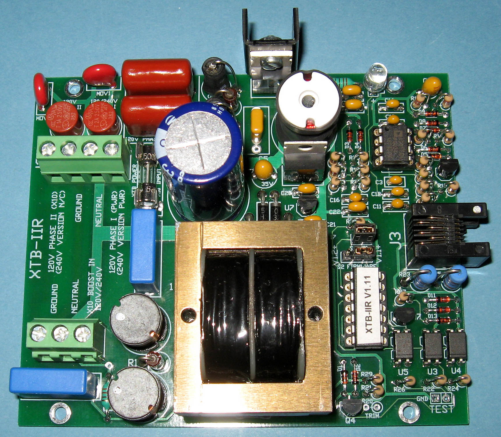
XTB-IIR Assembled PCB
JV Digital Engineering Home Page
[XTB & XTB-II/R Overview] [XTB Home Page] [XTB Ordering Info] [X10 Troubleshooting Info]