XTB-F10 Interconnections
XTB-F10 Assembly Notes
02/19/13 (Production version 1.0 PCB)
Please check for the latest version before beginning assembly.
The XTB-F10 is an easy PCB to assemble. One location was left open for a possible trim, but it is not presently used. The inductor locations have been reversed from the original units to provide slightly better performance when isolating a "signal sucker".
BEFORE ASSEMBLY
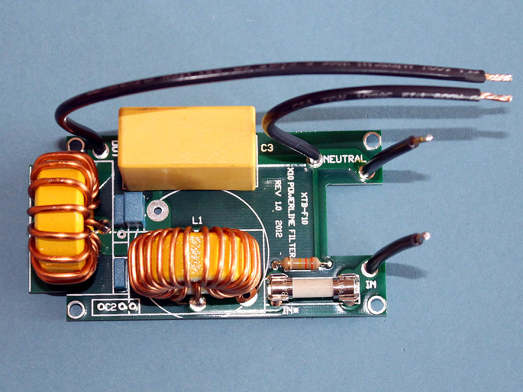
There are not many components used in the XTB-F10. The large inductors can be identified by the number of turns. More turns means higher inductance. The capacitors are marked with a code.
PRINTED CIRCUIT BOARD ASSEMBLY:
Please refer to the parts list, board layout, and high-resolution photograph of the assembled board while assembling your own unit:
XTB-F10 Version 1.0 Board Layout
XTB-F10 Version 1.0 Board Photograph
Things to watch out for:
1) These notes apply to the production version 1.0 PCB with the green solder mask. Contact me for the prior version of the assembly notes if you have the prototype PCBs without the solder mask.
2) There are duplicate traces on both sides of the PCB for all high-current paths. To minimize voltage drop in these runs, apply sufficient heat and solder to achieve a solid connection to the traces on both sides of the PCB. That may require removing a little more insulation on the inductor leads by abrading it with a pair of long-nose pliers
3) Make sure you are installing the inductors in the correct locations. While the values are not marked on the inductors, more turns means higher inductance.
RECOMMENDED ASSEMBLY ORDER:
R1
C1, C4, C5 (The .033uF can be installed at either C1 or C2.)
2 fuse clips (Orient so the fuse can snap in)
F1
Remove additional insulation from L1 & L2 as necessary for a good flow-through joint.
L1 & L2 (The inductor with more turns goes closest to the fuse.)
C3
INTERWIRING & FINAL ASSEMBLY:
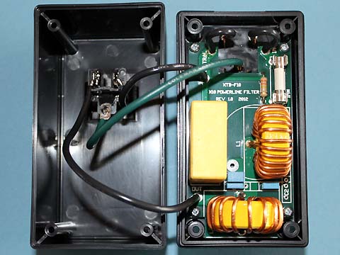
The AC receptacle should be pressed into the opening in the Polycase cover with the same alignment as the plug on the base. The receptacle may not lock in securely unless a screwdriver is used to force the plastic tabs slightly outward until they click into place.
Cut the black wire into two 2", one 4", and one 6" length. Strip 1/8" from one end and 1/4" from the other end of each wire. Solder the 1/8" ends to the PCB as shown in the photograph. The longest length is in the corner by the inductor. Since these wires may carry up to 10 amps, be sure that solder flows through the hole so a good connection is made to the PC traces on both the top and bottom.
The 5" green wire supplied with the kit will run directly between the ground pin on the plug and the ground tab on the socket. Strip 1/4" from one end and 1/2" from the other end. Insert the longer stripped end into the back of the plug ground pin. Crimp and solder, being careful not to overheat and soften the plastic.
Before mounting the PCB to the base, make sure all leads are cut within 1/16" of the bottom of the circuit board. Then mount the board to the base with the 4 short screws.
After the board is mounted, the AC connections are made as follows:
both 2" wires to the adjacent AC plug prongs
XTB-F10 Interconnections
Position the wires in the free space at the center of the PCB, and attach the cover to the base with the 4 long black screws.
Add the XTB-F10 label to the recessed portion on the back.
TEST & OPERATION:
Once assembled, plug it into an AC outlet and verify that it will power any load up to 10 amps that is plugged into the receptacle.
Please contact me if you have any questions at: jeff@jvde.us
If you don't receive a response within 24 hours, try: xtbjeff@gmail.com
JV Digital Engineering Home Page
[XTB & XTB-II/R Overview] [XTB Home Page] [XTB Ordering Info] [X10 Troubleshooting Info]